- The 16-Layer HBM3e chips are expected to roll-out in 2025
- New chips offer improved AI learning and inference capabilities
- Users can expect lower latency, Sk hynix claims
SK hynix has announced plans to add an additional four layers to its 12-HI HBM3e memory chips in a drive to bolster capacity.
The move will see the company increase capacity from 36GB to 48GB, and the semiconductor giant expects to begin distribution of sample products in early 2025.
The announcement could deliver significant performance improvements for organizations ramping up AI development. HBM3e chips have traditionally boasted a maximum of 12 layers, but with the advent of HBM4, users can glean greater performance.
Stacked and ready
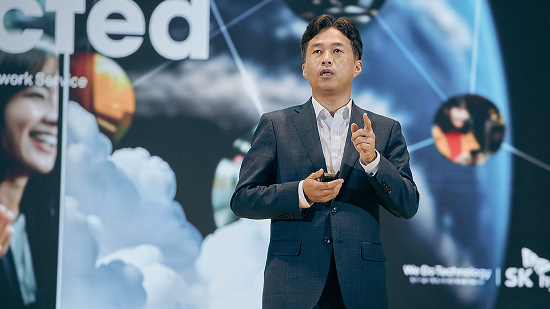
Company CEO Kwak Noh-Jung announced the launche during its recent SK AI Summit in Seoul, noting the upgrade will help markedly improve AI learning performance and inference capabilities.
“We stacked 16 DRAM chips to realize 48 GB capacity and applied Advanced MR-MUF technology proven for mass production. In addition, we are developing hybrid bonding technology as a backup process,” he said.
Kwak added initial in-house testing shows the 16-layer HBM3e can improve both AI learning and inference by 18% and 34% respectively compared to previous 12-layer HBM3e
“The 16-layer HBM3E is planned to be commercialized in 2025,” Kwak revealed.
HBM4 offers over 10 Gbps per pin compared to the high-end maximum of 9.2 Gbps offered by its predecessor. All told, this will unlock bandwidth capabilities of up to 1.5 TBps compared to HBM3e’s 1.2-plus TBps.
Moreover, manufacturers expect HBM4 will also deliver lower latency.
Under the hood of the 16-Hi product
In terms of design, the 16-Hi product has been developed using mass reflow-molded underfill (MR-MUF) technology. This next-generation tech can enable warp-free stacking of chips that are 40% thinner than conventional alternatives.
This also delivers improved heat dissipation due to the use of new protective materials, the company said.
Similarly, hybrid bonding has also unlocked marked improvements. This involves directly bonding chips without the need for forming a ‘bump’ between them during stacking, SK hynix noted.
“This reduces the overall thickness of the chip, enabling high stacking,” the company said in an announcement. “SK hynix is looking at both Advanced MR-MUF and hybrid bonding methods for 16-layer and higher HBM products.”


+ There are no comments
Add yours